


🎶 Unleash Your Creativity with Precision Waveforms!
The AD9834 DDS Generator Module is a cutting-edge device designed for generating high-performance sine, triangle, and square waves. With a 75 MHz clock rate and impressive modulation capabilities, it offers a resolution of 0.28 Hz at high speeds and 0.004 Hz at lower speeds. Its independent analog and digital sections ensure compatibility with various microcontrollers, while the sleep function minimizes power consumption, making it an economical choice for diverse applications in RF communication, sensor technology, and medical equipment.
T**S
Works well
Works as advertised, both sinewave and squarewave outputs. I did not try triangle waves. Above 1 MHz the sinewave is distorted, but that is expected.
C**S
Used and No Schematic
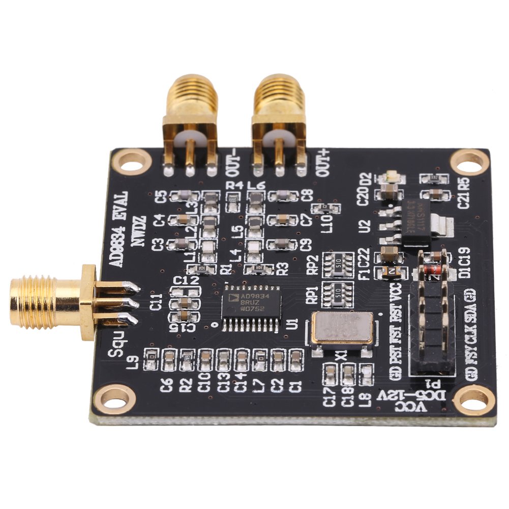
The board arrived sealed in antistatic plastic. No documentation or schematic was included. When I cut open the bag, I discovered the board was covered in dirt. It appears to have dropped in a mud puddle and left to dry before being sealed in the plastic.I rubbed off the dirt and discovered the Analog Device chip is a AD9834BRUZ and not the advertised AD9834CRUZ. The grade “B” part is only certified for 50 MHz. The board does contain a 75 MHz oscillator. Which means the board manufacture is running the DDS DAC 50% beyond design. I do not know why the board manufacture attempted to save money by using the cheaper grade of IC. The list price difference is only 99 cents on ADI’s web site.The board is marked for 5 to 12 VDC power input. There appears to be a regulator on the board. I was not able to rub the oily dirty off this IC and read its markings. I did power the board with 5 VDC and received a green LED power light.The board provides 10th inch header with the SPI signals, phase and frequency register selection, power, and ground. The board does not provide access to the SLEEP pin.The AD9834 provides a differential sinewave. The board provides this with two SMA connectors. One is labeled OUT+ and the other is labeled OUT-. There is a LRC network between the AD9834 pins and the SMA connectors. Without a schematic I do not know the purpose of this circuit. The two SMA outputs are designed to be hooked to a pair of power amplifiers and they would power both ends of a dipole antenna.I tested the output at various frequencies. To 18.75MHz you receive a 120 mV peak-to-peak signal. This drops to 60 mV p2p at 20 MHz, and the signal is all but gone 25 MHz (6 mV). The IC will not attempt to generate frequency above 37.5 MHz and shuts down the DDS. The SPI bus will clock up to 20 MHz.
O**.
Late and damaged
Late and damaged
Trustpilot
1 day ago
1 month ago